
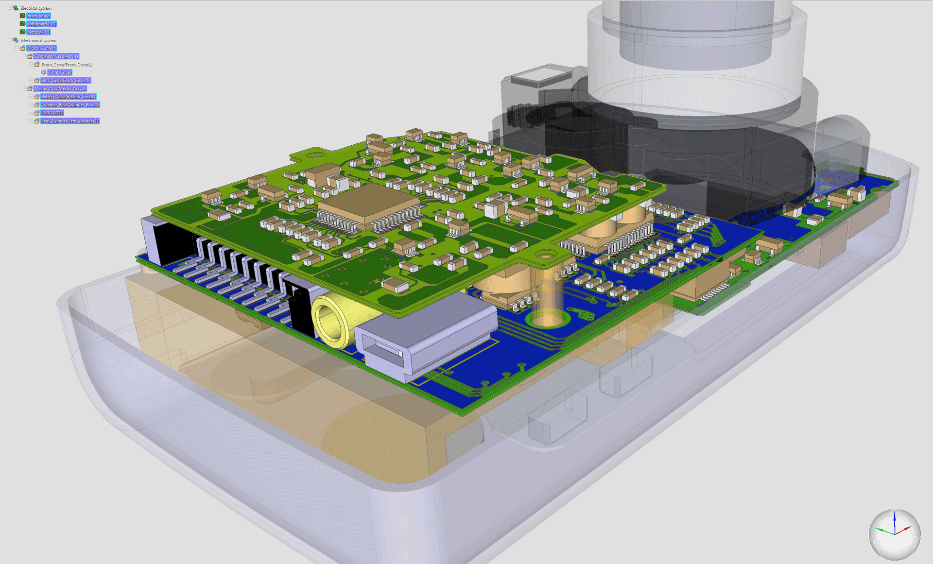

BOM Sourcing
BOM sourcing service refers to a service that assists in the procurement of Bill of Materials (BOM) components for manufacturing or product assembly.

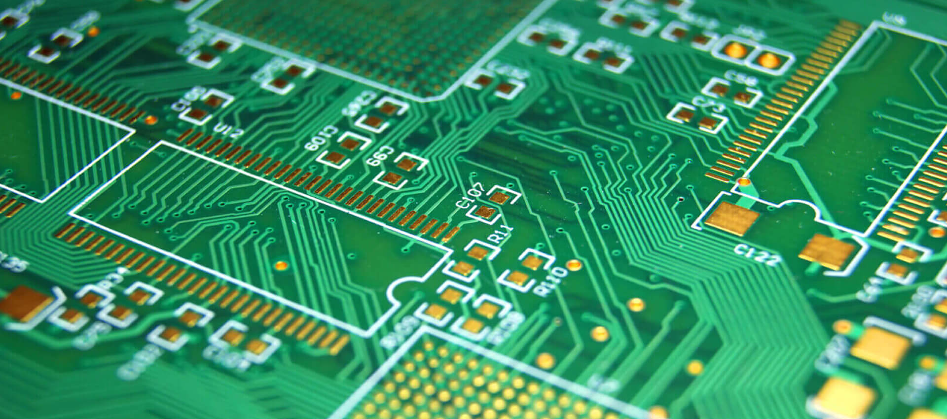
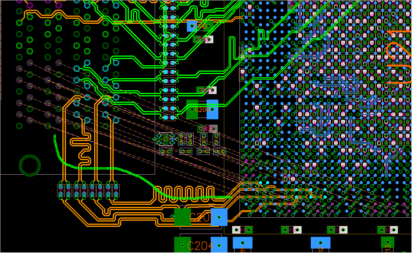
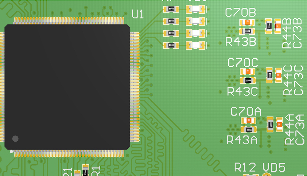
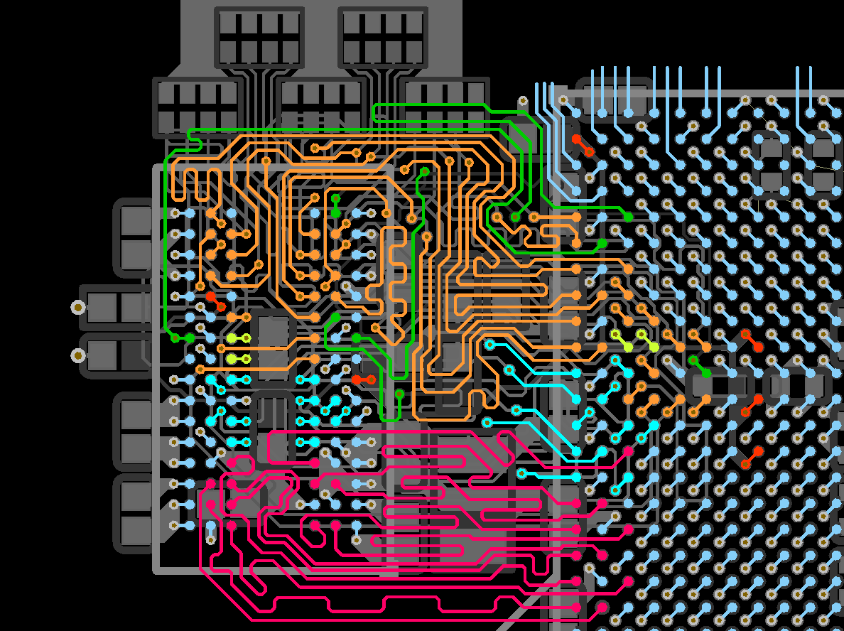
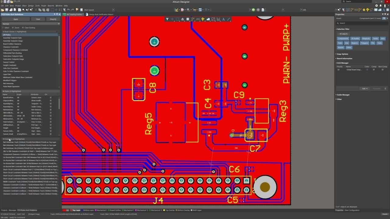
SMT PCB Assembly
SMT (Surface Mount Technology) PCB Assembly is a method of assembling electronic circuits on printed circuit boards (PCBs).

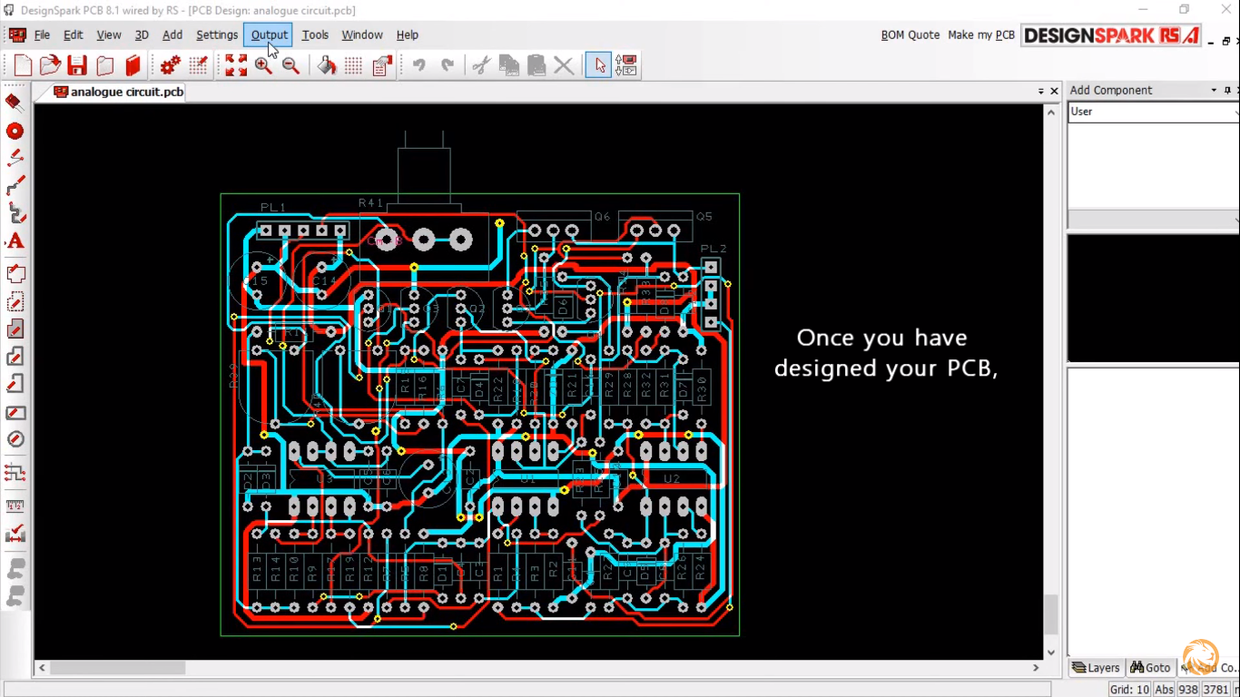
Through Hole Assembly
Through-hole PCB Assembly is a method of assembling electronic circuits on printed circuit boards (PCBs) using through-hole components.

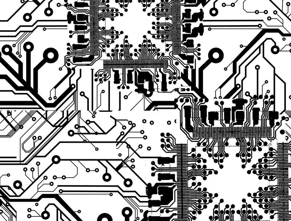
Turn Key PCB Assembly
Turnkey PCB Assembly service refers to a comprehensive service provided by a manufacturing company or assembly house where they handle...